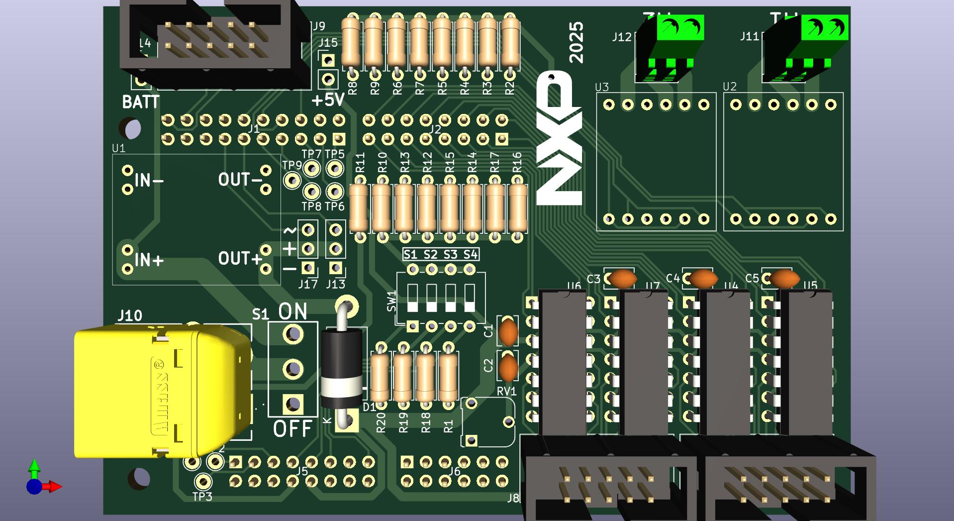
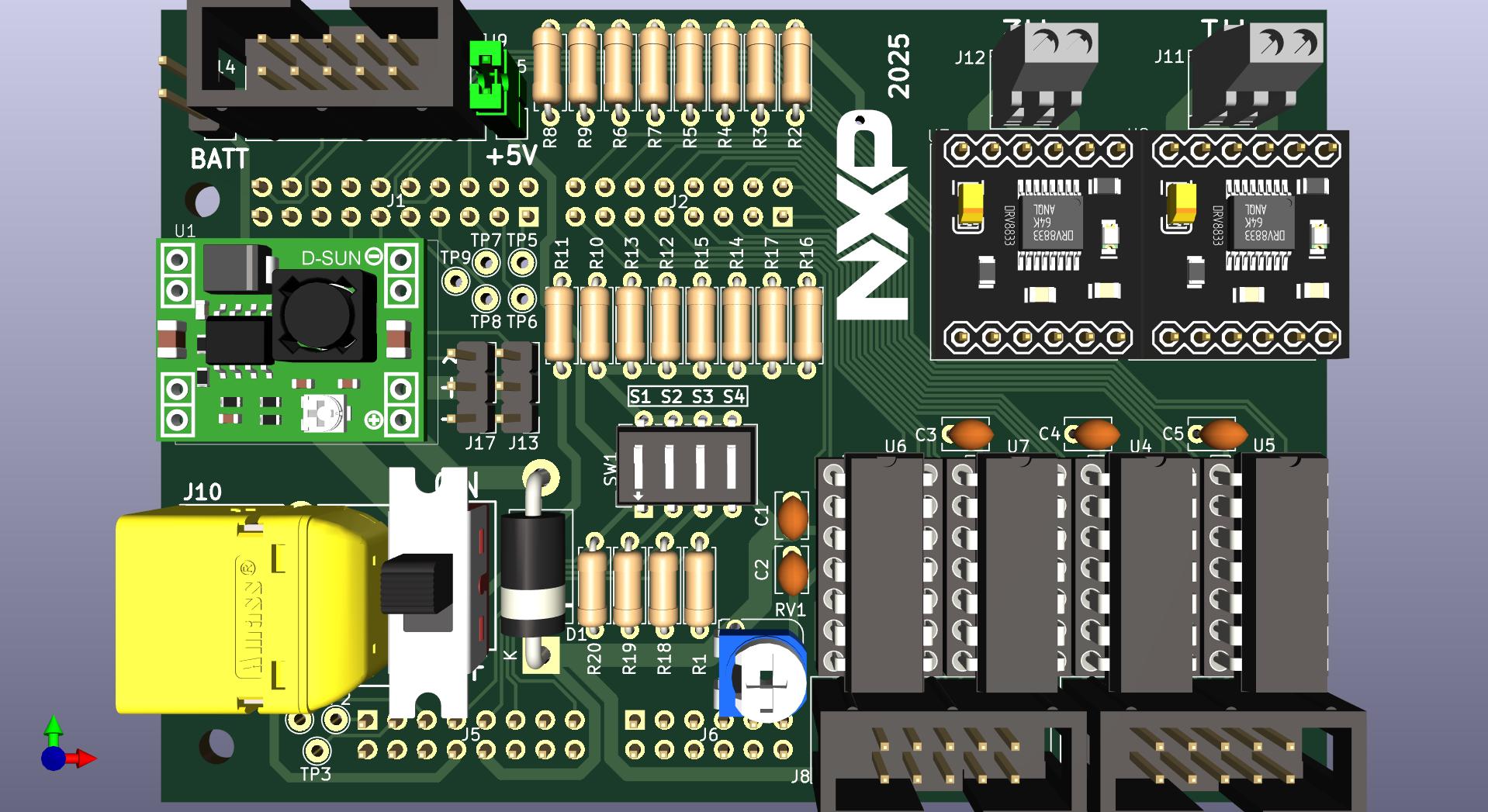
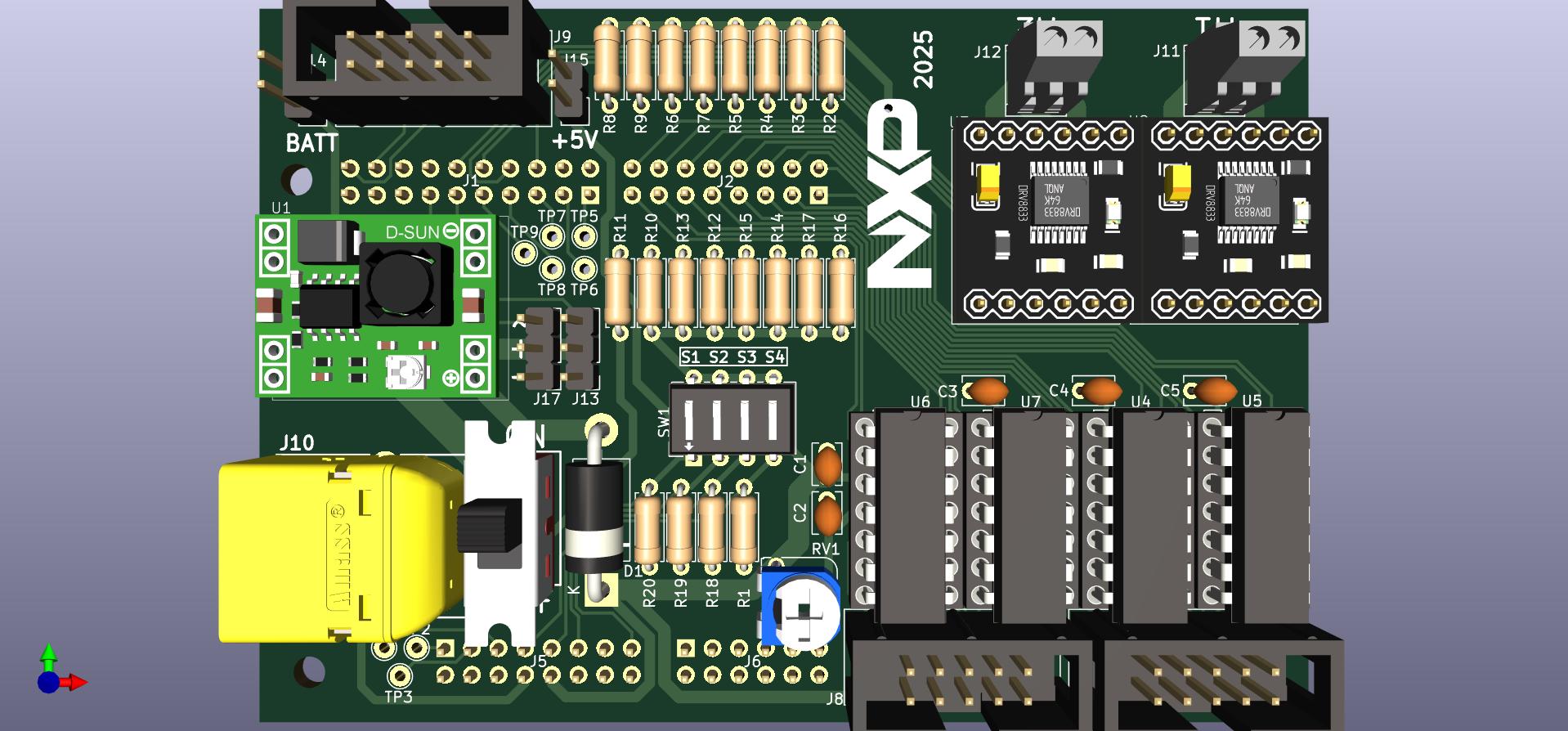
NXPCUP-Shield-FRDM-MCXN947 Assembly Guide
← Back to Main | ← Shield Components
Assembly Steps Overview
- Component Preparation
- Soldering Resistors
- Soldering Capacitors
- Soldering Diode
- Soldering IC Sockets
- Soldering Header Connectors
- Soldering JTAG Connectors
- Soldering XT60 Connector
- Soldering Screw Terminals
- Soldering 2-pin and 3-pin Connectors
- Soldering Potentiometer
- Soldering Switch
- Soldering DIP Switch
- Mounting DC-DC Converter
- Mounting Motor Drivers
- Inserting LM339 ICs
- Mounting Jumper
- Final Verification
- PCB Cleaning
Before You Begin
Safety Precautions
- Wear safety glasses when soldering
- Keep soldering iron in a safe stand when not in use
- Avoid touching the soldering iron tip
- Wash hands after handling solder (especially lead-based)
Soldering Tips
- Use appropriate temperature (300-350°C for lead-free solder)
- Clean the tip regularly on a damp sponge
- Apply solder to the joint, not the iron
- Heat both the pad and component lead
- Use just enough solder for a shiny, cone-shaped joint
- Allow joints to cool naturally (don't blow on them)
Step 1: Component Preparation
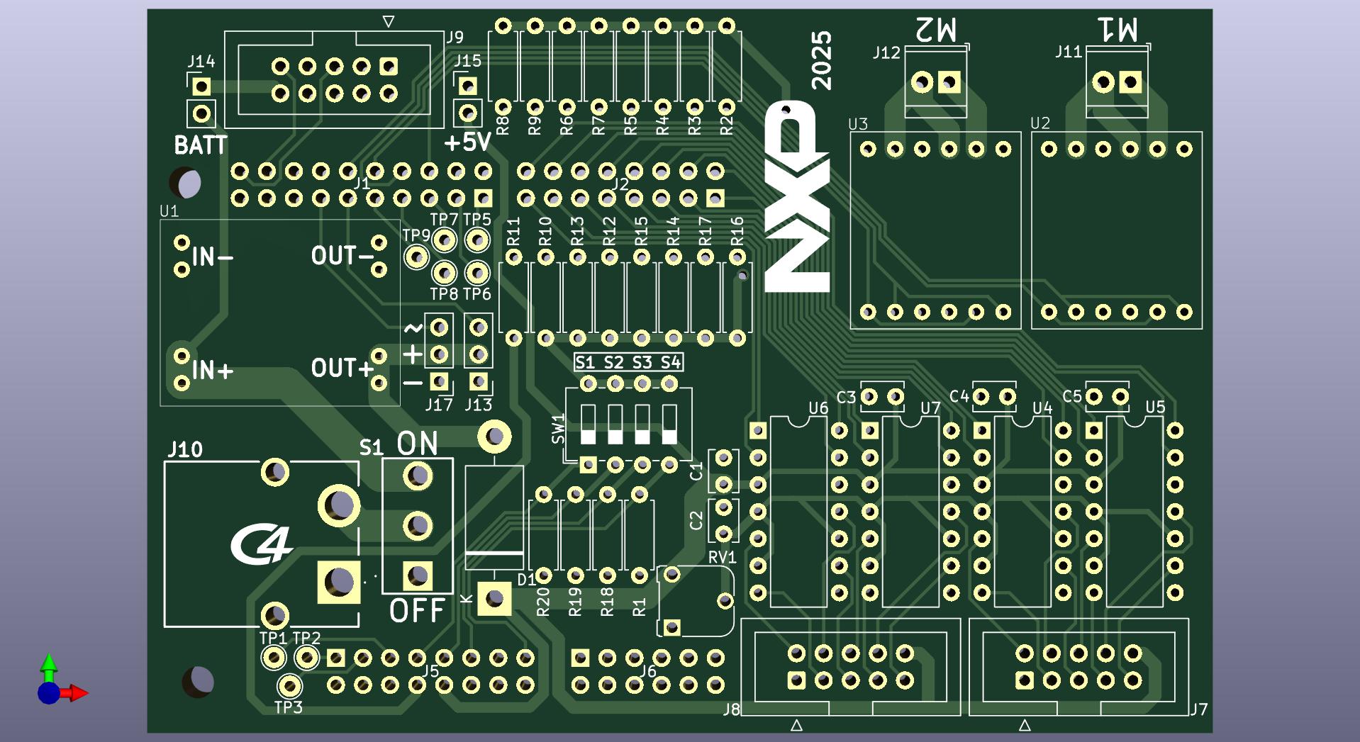
Checklist
Verify that you have all electronic components from the Shield Components table:
Organize Your Workspace
- Lay out all components in groups
- Label small containers for cut-off leads
- Have your tools ready and accessible
- Ensure good lighting
- Keep the PCB clean and free from debris
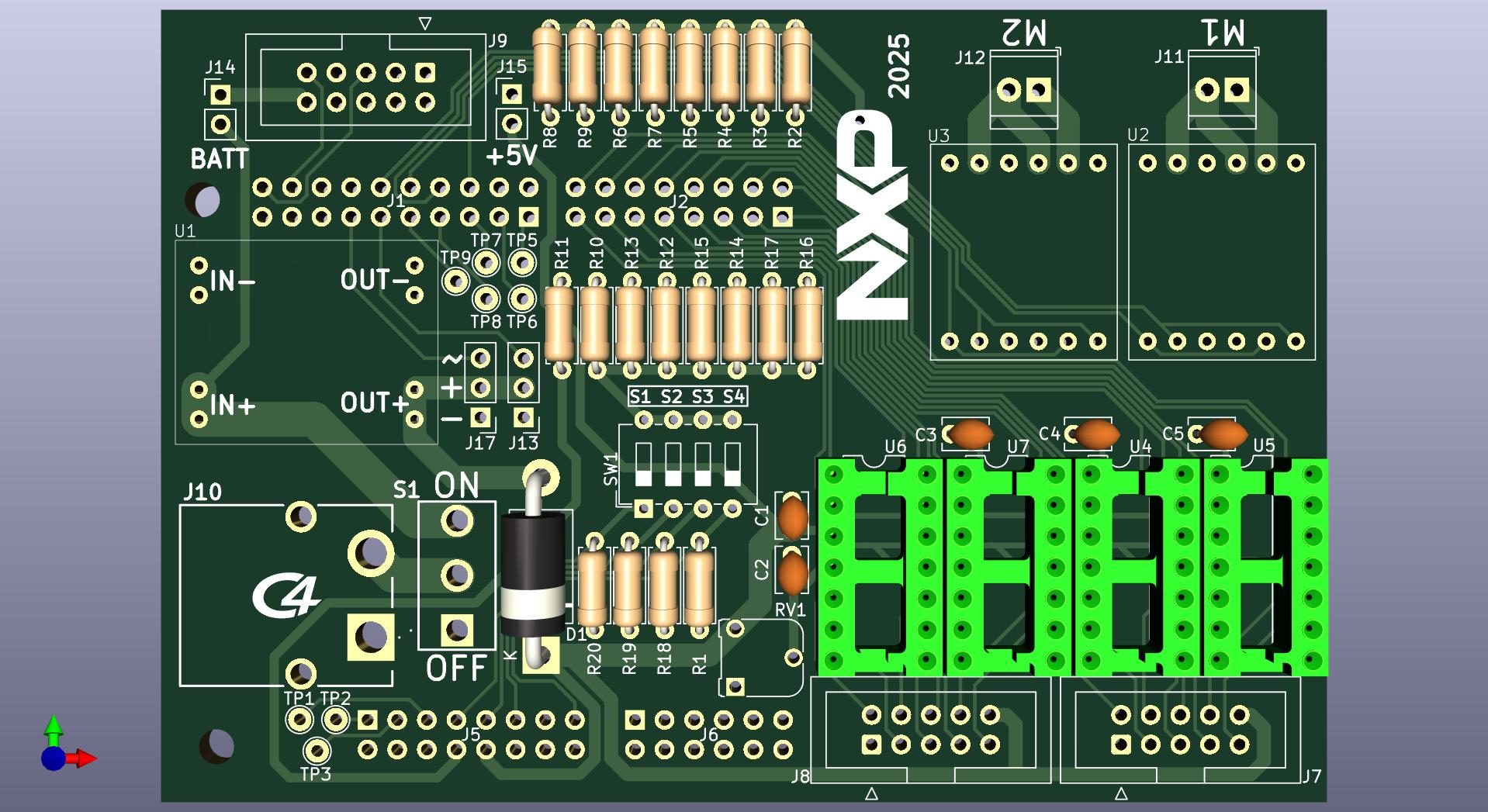
Step 2: Soldering Resistors (R1-R20)
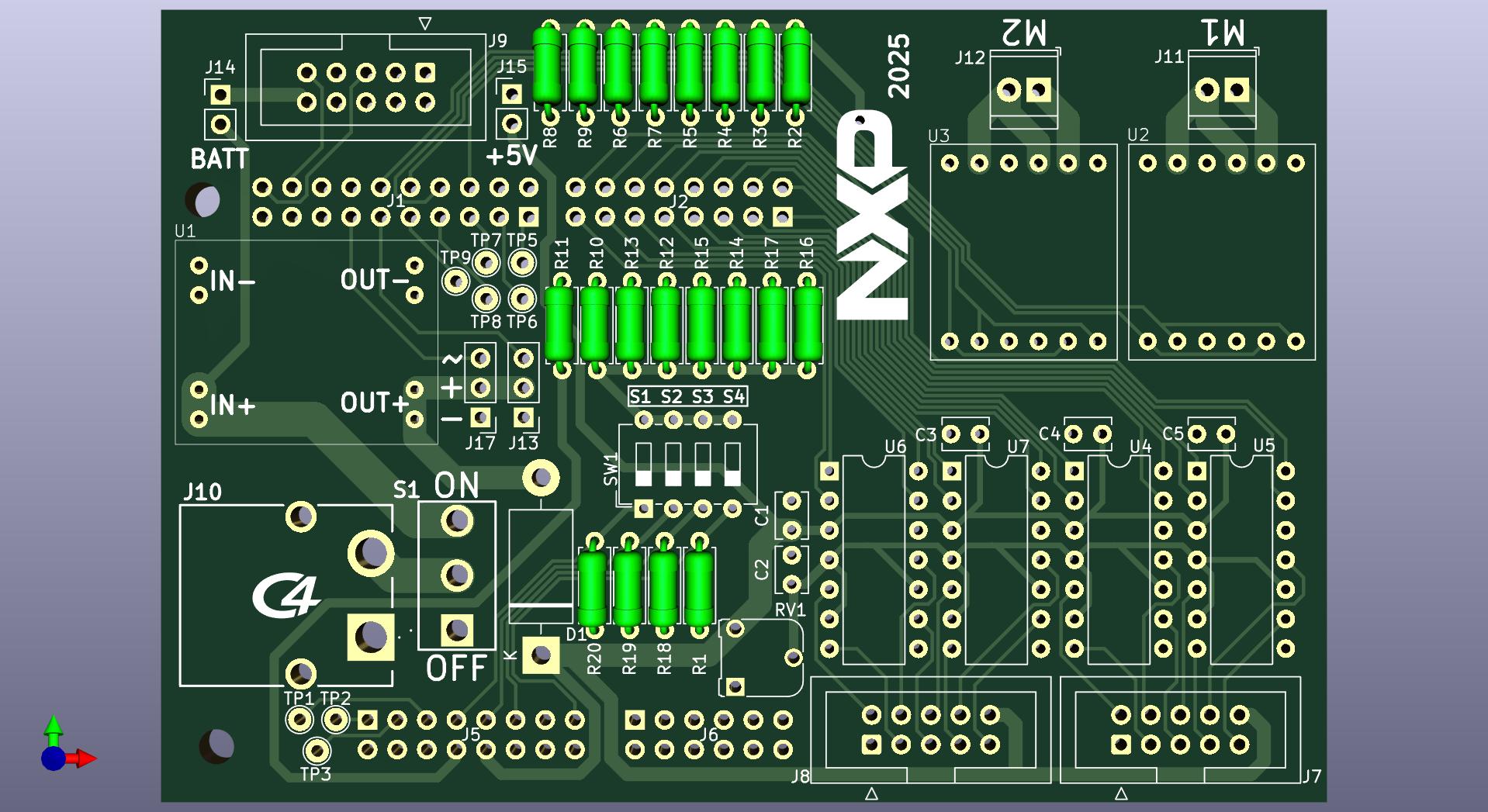
Instructions
- Identify positions R1-R20 on the PCB silkscreen
- Bend the leads:
- Use the resistor body width as a guide
- Bend leads at 90° directly next to the resistor body
- Insert resistors:
- Push through the PCB holes
- Resistors can be mounted in either direction (no polarity)
- Ensure the resistor body sits flush against the PCB
- Secure the component:
- Bend the leads slightly outward on the bottom to hold in place
- Solder the joints:
- Heat both the pad and the lead for 2-3 seconds
- Apply solder to create a shiny, cone-shaped joint
- Remove solder first, then the iron
- Trim excess leads:
- Use flush cutters to trim close to the solder joint
- Cut at a slight angle away from the joint
Quality Check
- All 20 resistors are soldered
- Solder joints are shiny and cone-shaped
- No cold solder joints (dull, grainy appearance)
- No solder bridges between adjacent pads
- Leads are trimmed flush
Note: Resistors have no polarity and can be mounted in any direction.
Step 3: Soldering Capacitors (C1-C5)
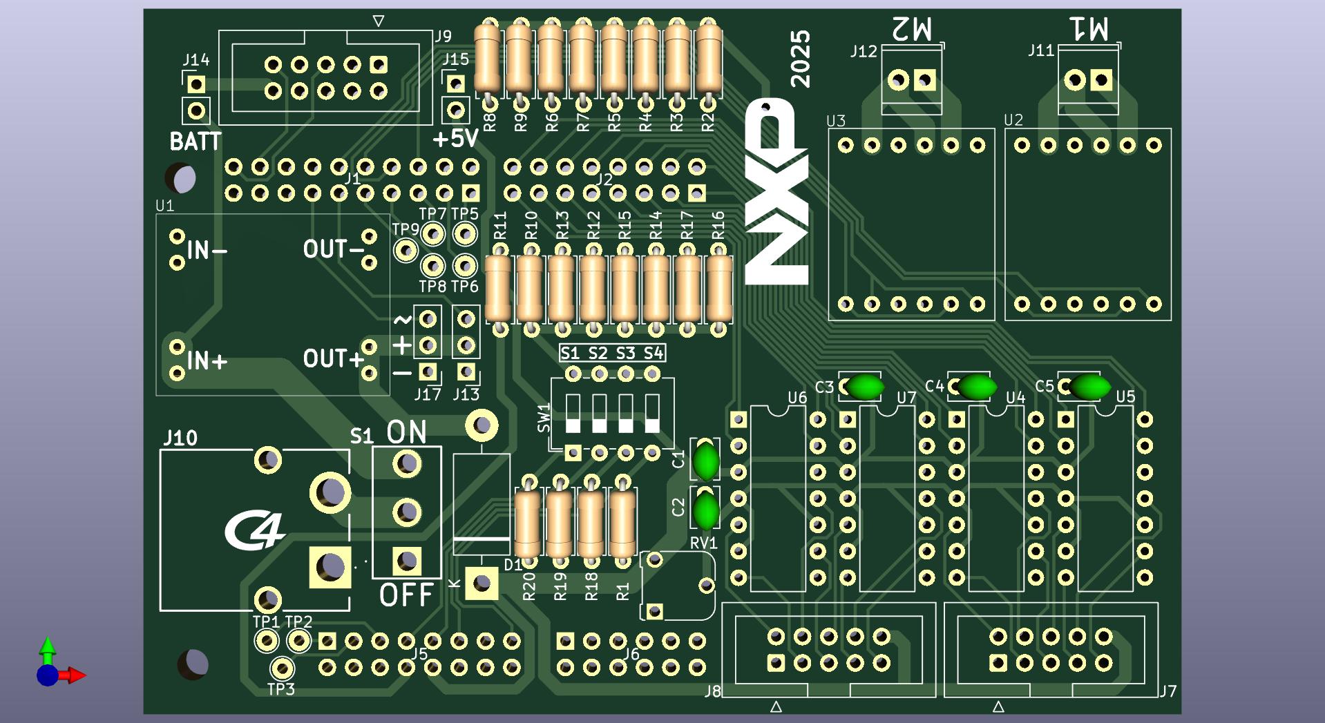
Instructions
- Identify positions C1-C5 on the PCB
- Insert capacitors:
- Ceramic capacitors have no polarity
- Insert leads through the marked holes
- Push until the capacitor body touches the PCB
- Secure and solder:
- Bend leads slightly on the bottom side
- Solder each lead using the same technique as resistors
- Trim excess leads:
- Cut flush with the solder joint
Quality Check
- All 5 capacitors are soldered
- Capacitors sit flat against the PCB
- Solder joints are clean and shiny
- No excess solder or bridges
Note: Ceramic capacitors have no polarity.
Step 4: Soldering Schottky Diode (D1)
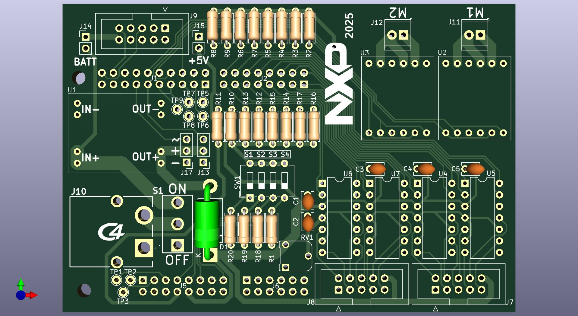
Instructions
- Identify position D1 on the PCB
- ⚠️ CHECK POLARITY:
- The diode has a band marking on one end (cathode)
- The PCB has a corresponding marking (usually a line or band)
- The band on the diode MUST match the marking on the PCB
- Insert the diode:
- Align the band with the PCB marking
- Double-check orientation before soldering
- Push the diode body close to the PCB
- Solder the leads:
- Solder both leads securely
- Trim excess leads
Quality Check
- Diode polarity is correct (band matches PCB marking)
- Both leads are soldered properly
- Diode body is close to PCB surface
⚠️ CRITICAL: Incorrect diode orientation will prevent the circuit from working and may cause damage!
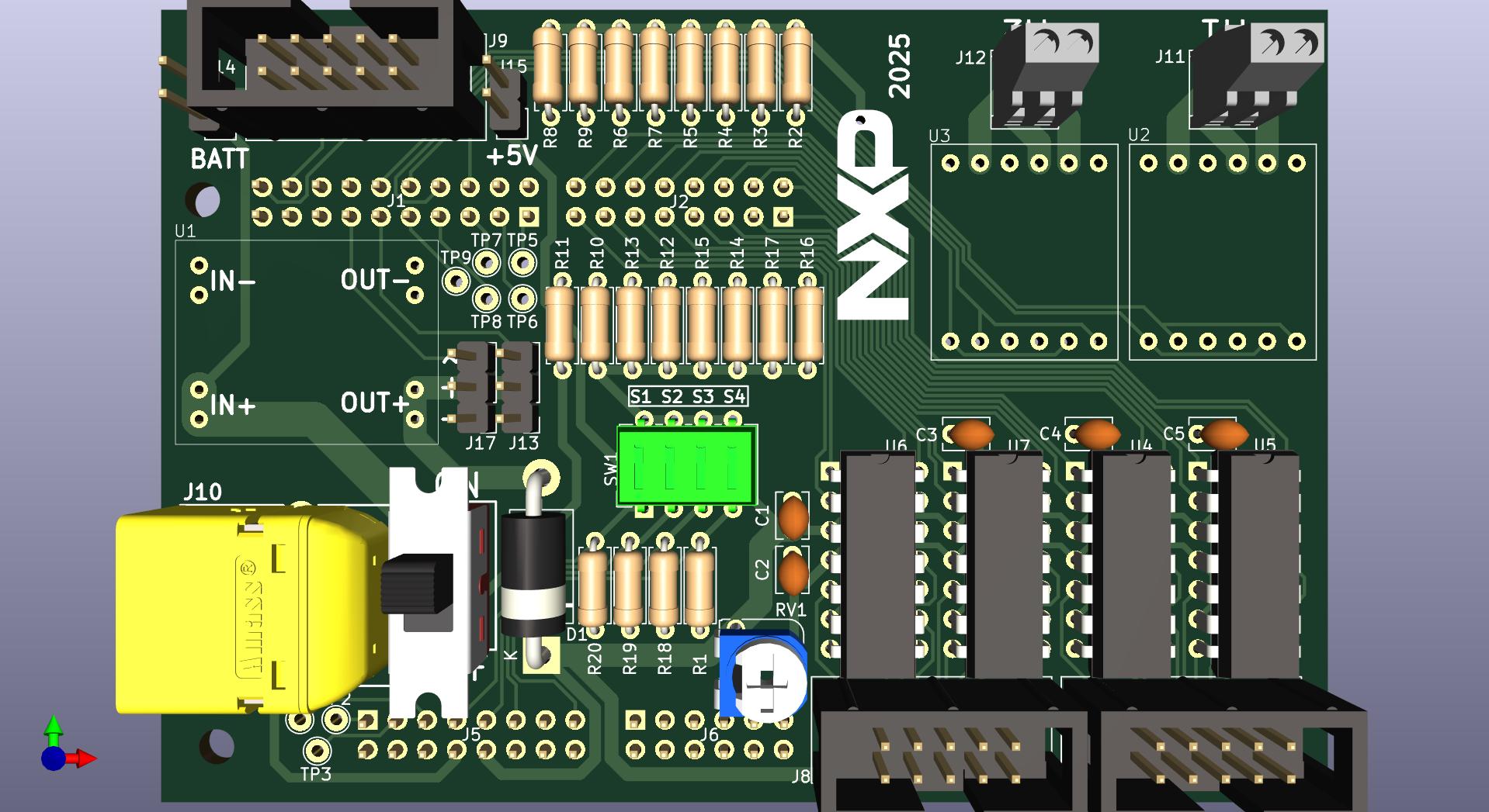
Step 5: Soldering IC Sockets (for U4-U7)
Instructions
- Identify positions U4-U7 on the PCB
- Orient the sockets:
- Each socket has a notch or dot indicating pin 1
- Match this with the marking on the PCB
- ⚠️ Correct orientation is critical!
- Insert sockets:
- Place socket into the PCB holes
- Ensure all pins go through the holes (check for bent pins)
- Socket should sit flat against the PCB
- Secure the socket:
- You can tape the socket in place or use helping hands
- Solder one corner pin first
- Check alignment, reheat if needed to adjust
- Solder all pins:
- Solder the opposite corner pin
- Then solder all remaining pins (14 pins per socket)
- Ensure each pin has a good solder joint
Quality Check
- All 4 sockets (U4-U7) are installed
- Socket notches match PCB markings
- Sockets sit flat and perpendicular to PCB
- All 56 pins (14 pins × 4 sockets) are soldered
- No solder bridges between pins
Note: Do NOT insert the LM339 integrated circuits into the sockets yet. This will be done in Step 16.
Step 6: Soldering Header Connectors (J1, J2, J5, J6)
J1 - 2x10 Pin Connector
- Identify position J1 on the PCB
- Insert the connector:
- Align all 20 pins with the holes
- Ensure the connector is perpendicular to the PCB
- The plastic base should sit flush on the PCB
- Secure the connector:
- Solder one corner pin
- Check alignment and adjust if needed
- Solder the opposite corner pin
- Solder all pins:
- Solder all remaining 18 pins
- Ensure good solder flow on each pin
J2, J5 - 2x8 Pin Connectors
- Identify positions J2 and J5
- Insert each connector (16 pins per connector)
- Solder using the same technique:
- Corner pins first for alignment
- Then all remaining pins
J6 - 2x6 Pin Connector
- Identify position J6
- Insert the connector (12 pins)
- Solder all pins
Quality Check
- J1 (2x10) is soldered - 20 pins
- J2 (2x8) is soldered - 16 pins
- J5 (2x8) is soldered - 16 pins
- J6 (2x6) is soldered - 12 pins
- All connectors are perpendicular to PCB
- No solder bridges between pins
- All pins have good solder joints
Tip: These connectors will mate with the FRDM-MCXN947 board, so proper alignment is crucial.
Step 7: Soldering JTAG Connectors (J7-J9)
Instructions
- Identify positions J7, J8, J9 on the PCB
- Check orientation:
- JTAG connectors typically have a pin 1 indicator
- Match this with the PCB marking (usually a square pad or marking)
- Insert connectors:
- Each connector has 2x5 pins (10 pins total)
- Ensure all pins align with holes
- Connectors should be perpendicular to the PCB
- Solder each connector:
- Solder one corner pin first
- Check alignment
- Solder opposite corner
- Solder all remaining pins (10 pins per connector)
Quality Check
- All 3 JTAG connectors (J7-J9) are installed
- Pin 1 orientation is correct on each
- Connectors are perpendicular to PCB
- All 30 pins (10 pins × 3 connectors) are soldered
- No solder bridges
Note: J7 and J8 are used for line sensor connections, J9 is used for camera connection.
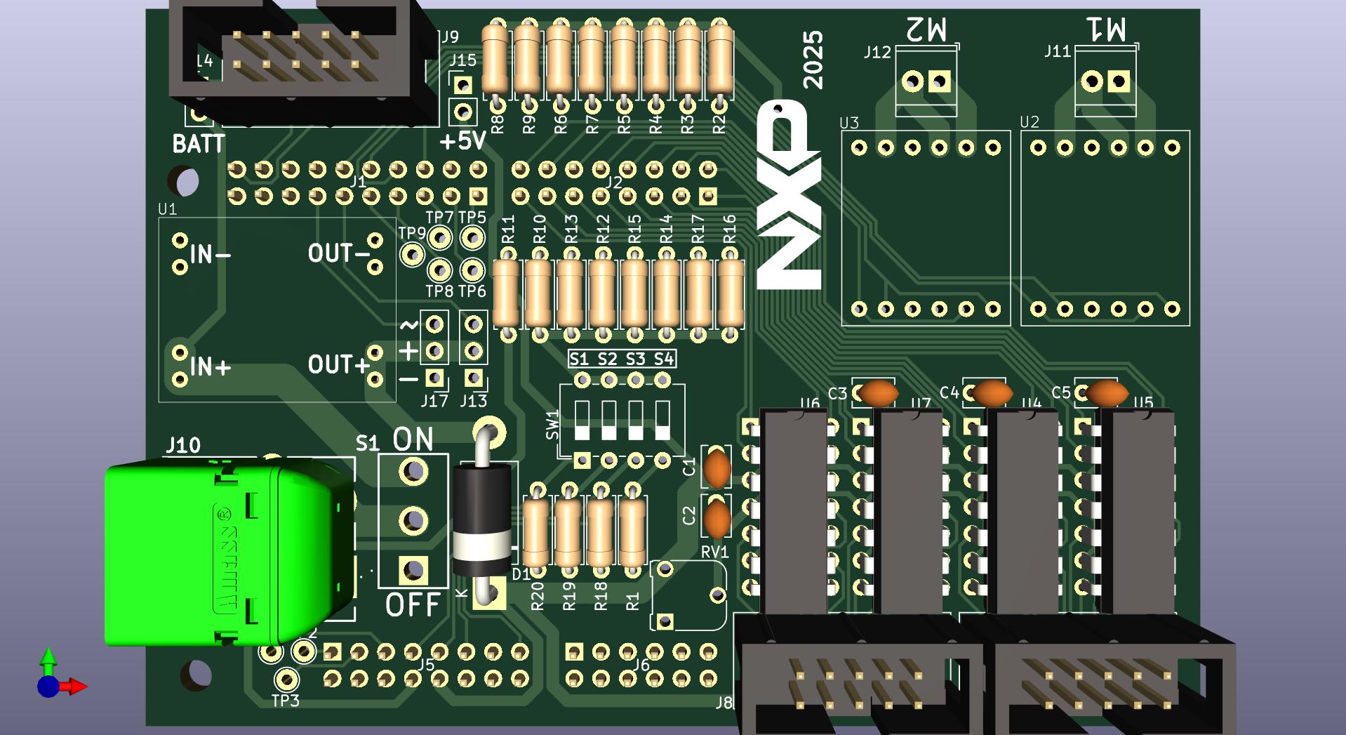
Step 8: Soldering XT60 Connector (J10)
Instructions
- Identify position J10 on the PCB
- ⚠️ CHECK POLARITY:
- XT60 connectors have + (positive) and - (negative) markings
- The PCB will have corresponding markings
- Verify correct orientation before soldering!
- Insert the connector:
- Align the connector with the PCB holes
- Ensure it sits flush against the PCB
- The connector body should be stable
- Solder the pins:
- XT60 pins are large and require more heat
- Heat the pin and pad for 3-5 seconds
- Apply sufficient solder for a strong joint
- Both pins must be solidly soldered
Quality Check
- XT60 connector polarity is correct (+ and - match PCB)
- Connector sits flush on PCB
- Both pins have strong, shiny solder joints
- No cold solder joints (these carry high current)
⚠️ CRITICAL: This connector carries battery power. Incorrect polarity or poor solder joints can cause serious damage or fire hazard!
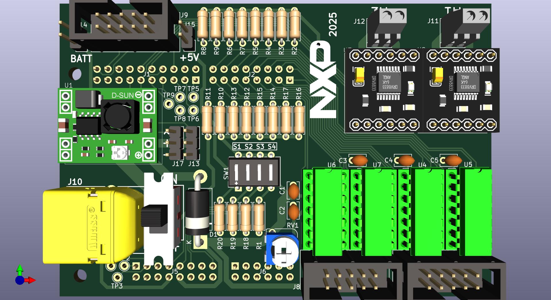
Step 9: Soldering Screw Terminals (J11, J12)
Instructions
- Identify positions J11 and J12 on the PCB
- Orient the terminals:
- The screw holes should face outward (away from the PCB center)
- This allows easy access for connecting motor wires
- Insert terminals:
- Push the pins through the PCB holes
- Ensure the terminal body sits flat on the PCB
- Solder the pins:
- Solder each pin (2 pins per terminal)
- These terminals carry motor current, so ensure good joints
Quality Check
- Both screw terminals (J11, J12) are installed
- Screw holes face outward for easy access
- All 4 pins (2 per terminal) are soldered
- Terminals sit flat on PCB
Note: These terminals will connect to the DC motors.
Step 10: Soldering 2-pin and 3-pin Connectors (J13-J15, J17)
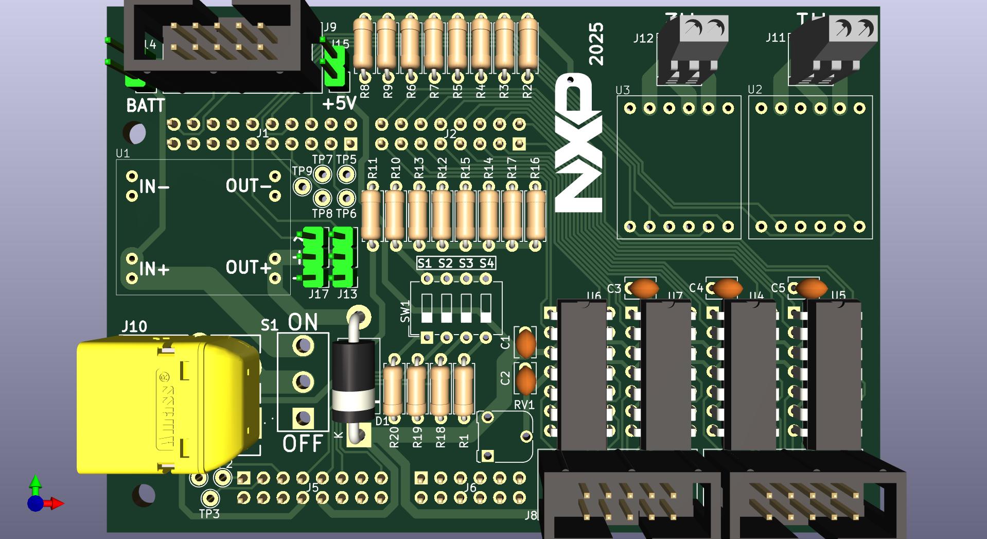
Instructions
- Identify positions:
- J13: 3-pin connector
- J14: 2-pin connector
- J15: 2-pin connector
- J17: 3-pin connector
- Insert each connector:
- Align pins with PCB holes
- Ensure connectors are perpendicular
- Solder all pins:
- J13: 3 pins
- J14: 2 pins
- J15: 2 pins
- J17: 3 pins
Quality Check
- J13 (3-pin) is soldered
- J14 (2-pin) is soldered
- J15 (2-pin) is soldered
- J17 (3-pin) is soldered
- All connectors are perpendicular to PCB
- Total 10 pins soldered
Step 11: Soldering Potentiometer (RV1)
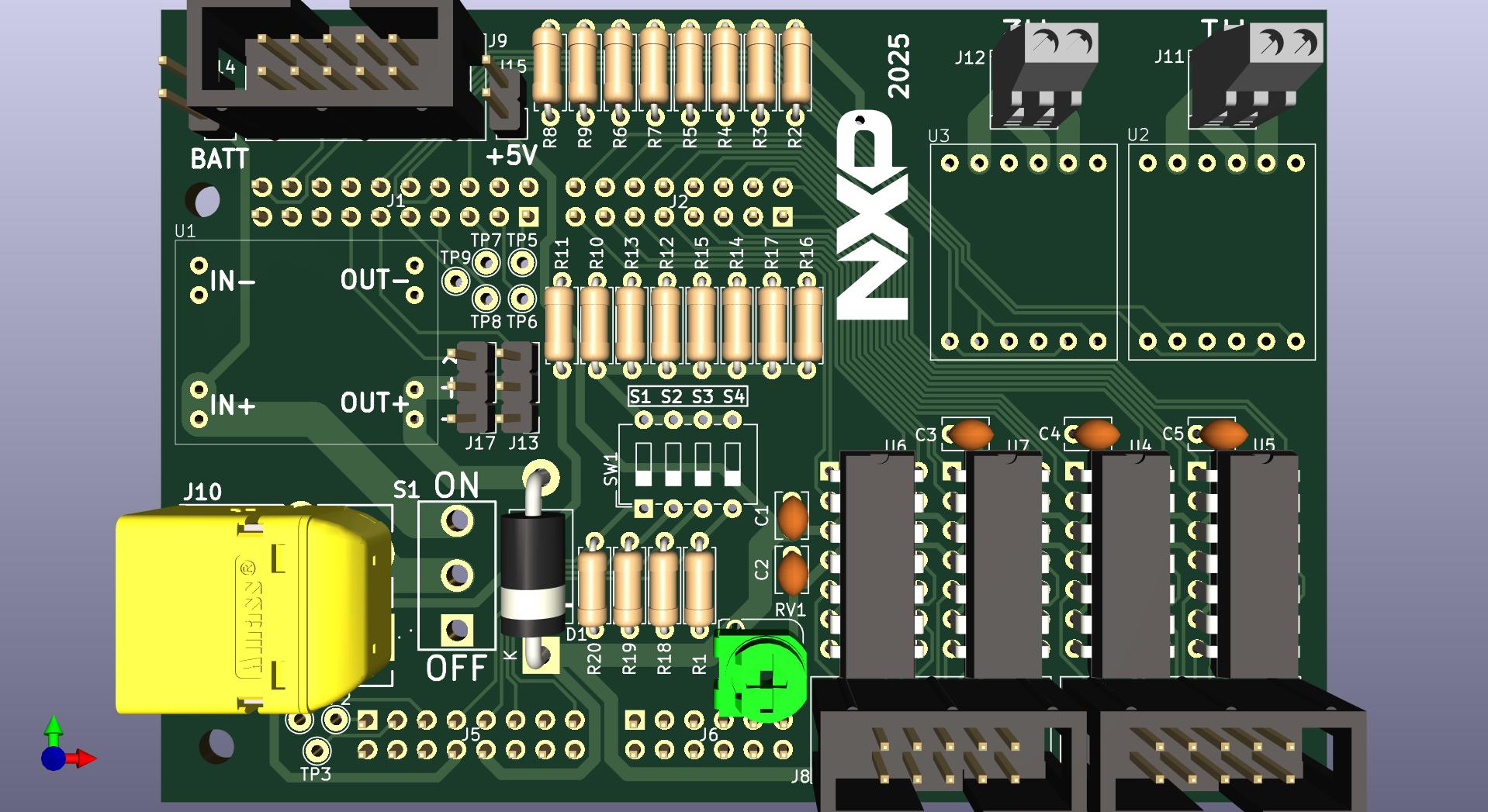
Instructions
- Identify position RV1 on the PCB
- Insert the potentiometer:
- Align the 3 pins with the PCB holes
- The adjustment screw should be accessible
- Push until the body sits on the PCB
- Solder the 3 pins:
- Ensure good solder joints on all pins
Quality Check
- Potentiometer is installed at RV1
- All 3 pins are soldered
- Adjustment screw is accessible
- Component sits flat on PCB
Note: This potentiometer adjusts the line sensor detection threshold.
Step 12: Soldering Switch (S1)
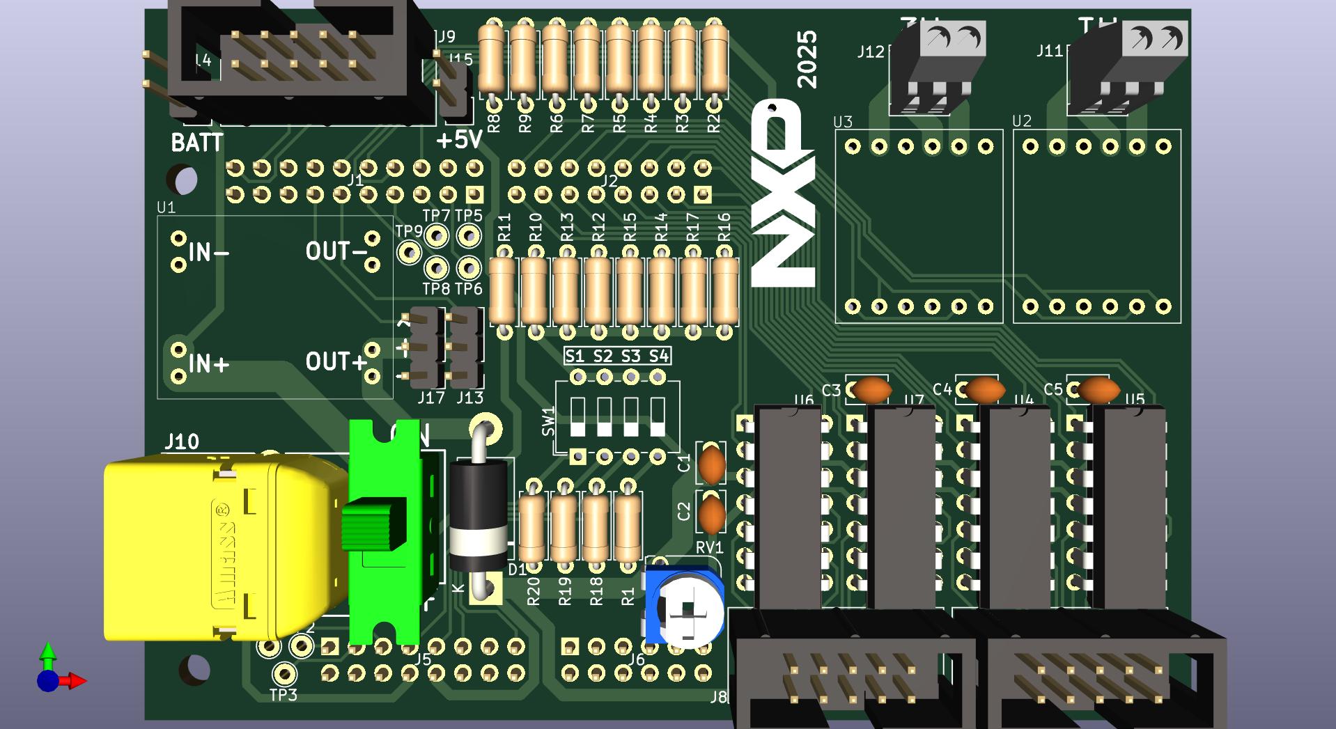
Instructions
- Identify position S1 on the PCB
- Insert the slide switch:
- Align the pins with the PCB holes
- Ensure correct orientation
- The switch should sit flat on the PCB
- Solder all pins:
- Solder each pin securely
- This is the main power switch, so good joints are important
Quality Check
- Switch is installed at S1
- All pins are soldered
- Switch operates smoothly
- Switch sits flat on PCB
Note: This is the main power on/off switch for the shield.
Step 13: Soldering DIP Switch (SW1)
Instructions
- Identify position SW1 on the PCB
- Check orientation:
- DIP switches usually have a marking for position 1
- Match this with the PCB marking
- Insert the DIP switch:
- Align all 8 pins with the PCB holes
- Ensure the switch sits flat
- Solder all 8 pins:
- Solder one corner pin first
- Check alignment
- Solder remaining pins
Quality Check
- DIP switch is installed at SW1
- Correct orientation (position 1 marked)
- All 8 pins are soldered
- Switch sits flat on PCB
- All 4 switches operate smoothly
Note: This 4-position DIP switch is used for configuration settings.(keep position 3 in ON state, do not use)
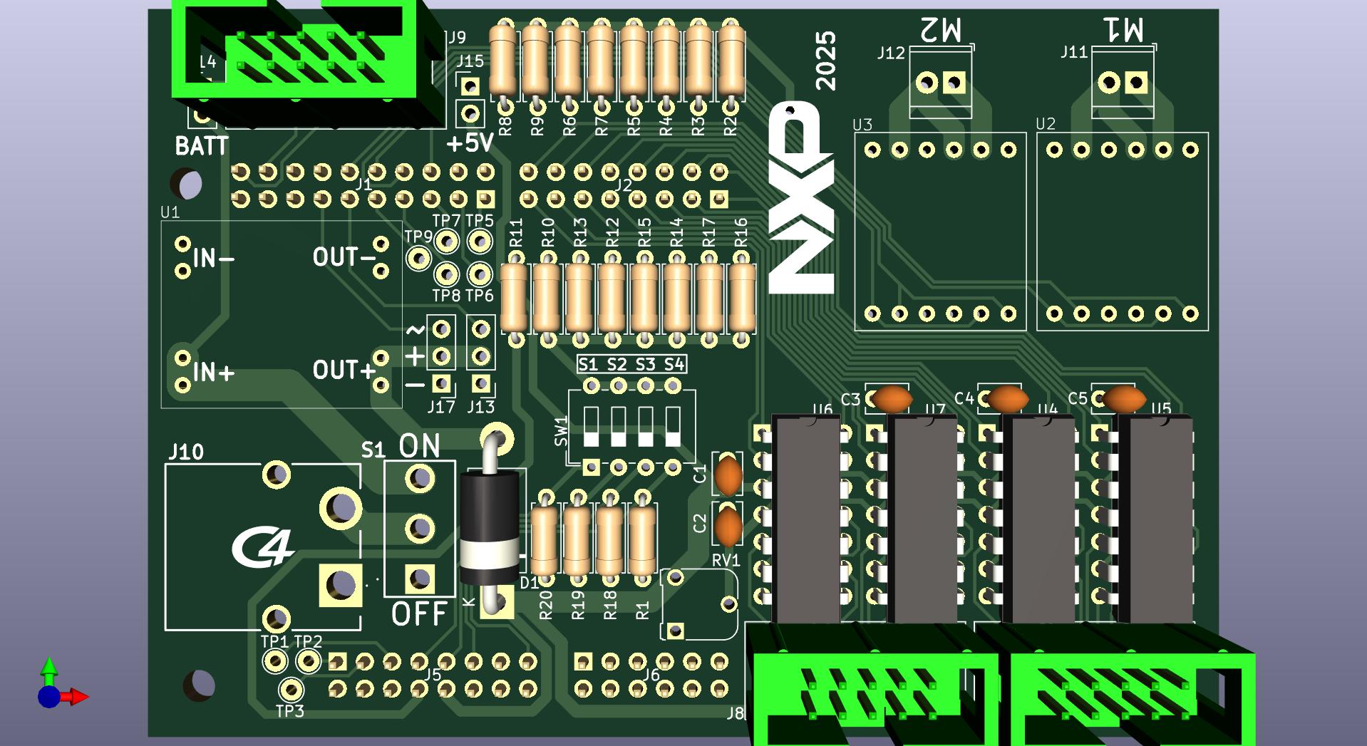
Step 14: Mounting DC-DC Converter (U1)
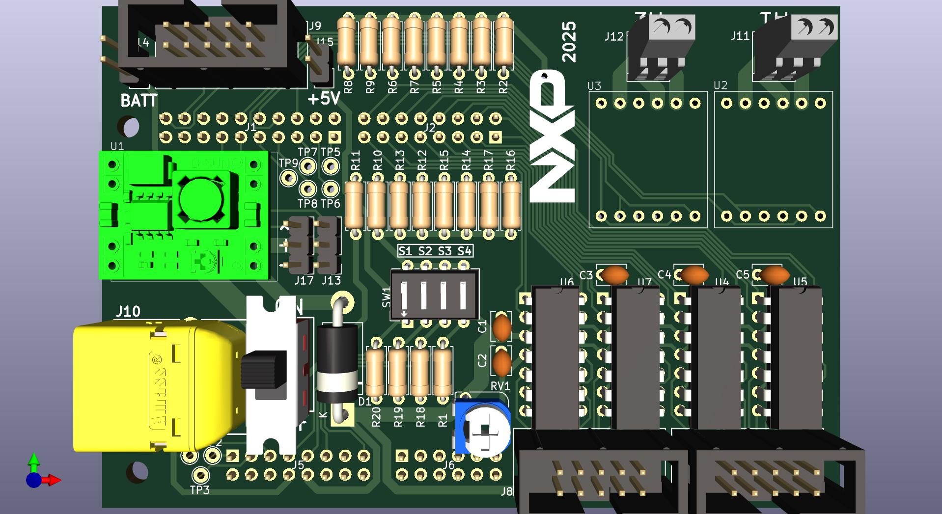
Instructions
- Identify position U1 on the PCB
- Prepare the MP1584EN module:
- Check the module pinout: IN+, IN-, OUT+, OUT-
- ⚠️ Verify connections before soldering!
- Position the module:
- Align the module pins with the PCB pads
- Ensure correct orientation (IN+ to IN+, etc.)
- The module should sit flat or at the designated height
- Connection between power source and shield is made through 4 connectors of 2 pins each
- Solder the connections:
- Solder IN+ pin
- Solder IN- pin
- Solder OUT+ pin
- Solder OUT- pin
- Use sufficient solder for good electrical and mechanical connection
- Adjust output voltage (if needed):
- Before final assembly, you may need to adjust the output voltage
- Use the onboard potentiometer on the MP1584EN
- Set to 5V output (measure with multimeter)
- ⚠️ Verify voltage before mounting any chips or connecting shield to FRDM board!
Quality Check
- MP1584EN module is installed at U1
- Correct orientation (IN+, IN-, OUT+, OUT- match PCB)
- All 4 connections are soldered (4 connectors of 2 pins each)
- Output voltage is set to 5V (if adjustable)
- Module is mechanically secure
⚠️ IMPORTANT: This module converts battery voltage (7.4V) to 5V for the logic circuits. Incorrect wiring can damage components!
Step 15: Mounting Motor Drivers (U2, U3)
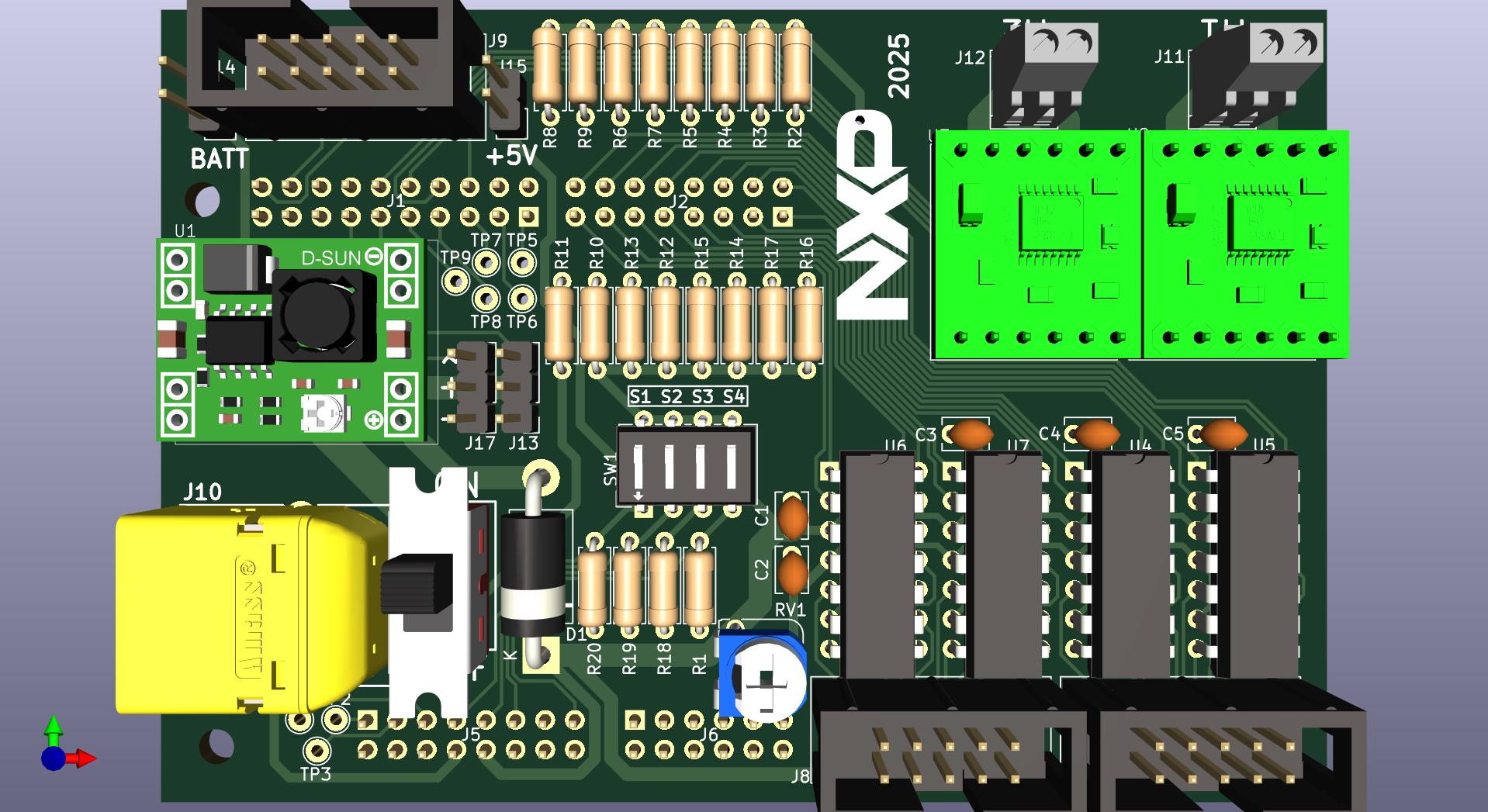
Instructions
- Identify positions U2 and U3 on the PCB
- Prepare the DRV8833 modules:
- Each module is a dual H-bridge motor driver
- Check the pinout on the module
- Identify: VCC, GND, IN1, IN2, IN3, IN4, OUT1, OUT2, OUT3, OUT4
- Position the first module (U2):
- Align all pins with the PCB pads
- ⚠️ Verify correct orientation!
- Ensure the module sits flat or at the correct height
- Solder all pins for U2:
- Solder one corner pin first
- Check alignment
- Solder all remaining pins
- Repeat for the second module (U3):
- Same procedure as U2
- Verify connections:
- Check that power pins (VCC, GND) are correctly connected
- Check that control pins (IN1-IN4) match the PCB design
- Check that output pins (OUT1-OUT4) go to motor terminals
Quality Check
- DRV8833 module is installed at U2
- DRV8833 module is installed at U3
- Both modules have correct orientation
- All pins are soldered on both modules
- No solder bridges between pins
- Modules are mechanically secure
Note: These drivers control the DC motors. U2 controls one motor, U3 controls the other.
Step 16: Inserting LM339 Integrated Circuits (U4-U7)
Instructions
- Prepare the LM339 ICs:
- Take the 4 LM339 quad comparator ICs
- ⚠️ Handle with care - these are static sensitive!
- Each IC has 14 pins
- Check IC orientation:
- Each LM339 has a notch or dot marking pin 1
- The IC sockets (U4-U7) also have notch markings
- The notch on the IC MUST match the notch on the socket
- Prepare IC pins (if needed):
- IC pins may be slightly splayed outward
- Gently bend pins inward by pressing the IC sideways on a flat surface
- Pins should be perpendicular to the IC body
- Insert the first IC (U4):
- Align the IC notch with the socket notch
- Align all 14 pins with the socket holes
- Press down gently but firmly
- All pins should enter the socket
- Do not force! If a pin bends, remove the IC and straighten the pin
- Verify insertion:
- The IC should sit flat in the socket
- No pins should be bent or outside the socket
- Repeat for U5, U6, and U7:
- Same procedure for each IC
- Always check notch orientation!
Quality Check
- LM339 IC is inserted in socket U4 (notch aligned)
- LM339 IC is inserted in socket U5 (notch aligned)
- LM339 IC is inserted in socket U6 (notch aligned)
- LM339 IC is inserted in socket U7 (notch aligned)
- All ICs sit flat in their sockets
- No bent pins
- All pins are in the socket (none outside)
⚠️ CRITICAL: Incorrect IC orientation will prevent the circuit from working and may damage the IC when powered!
Step 17: Mounting Jumper
Instructions
- Identify the jumper position on the PCB
- Locate connector J15 on the PCB
- This jumper selects the camera power source
- Mount the jumper:
- Place the jumper on J15
- The jumper connects two adjacent pins
- Verify configuration:
- Jumper on J15 selects 5V power for the camera (J9)
- This is the recommended configuration
Quality Check
- Jumper is installed on J15
- Jumper configuration is correct (5V camera power)
Note: The jumper on J15 provides 5V power to the camera connector (J9).
Step 18: Final Verification
Visual Inspection
-
Component check:
- All resistors (R1-R20) are installed
- All capacitors (C1-C5) are installed
- Diode D1 is installed with correct polarity
- All IC sockets (U4-U7) are installed with correct orientation
- All header connectors (J1, J2, J5, J6) are installed
- All JTAG connectors (J7-J9) are installed
- XT60 connector (J10) is installed with correct polarity
- Screw terminals (J11, J12) are installed
- All auxiliary connectors (J13-J15, J17) are installed
- Potentiometer (RV1) is installed
- Switch (S1) is installed
- DIP switch (SW1) is installed
- DC-DC converter (U1) is installed with correct orientation
- Motor drivers (U2, U3) are installed with correct orientation
- LM339 ICs are inserted in sockets with correct orientation
- Jumper is installed
-
Solder joint inspection:
- All solder joints are shiny (not dull or grainy)
- All joints have a cone shape (not ball-shaped or flat)
- No cold solder joints
- No solder bridges between adjacent pins or pads
- No excess solder creating blobs
- All component leads are trimmed flush
-
Component orientation check:
- Diode D1 band matches PCB marking
- IC socket notches match PCB markings
- LM339 IC notches match socket notches
- XT60 connector polarity is correct
- DIP switch position 1 is correctly oriented
- DC-DC converter IN/OUT connections are correct
- Motor driver modules are correctly oriented
Electrical Verification with Multimeter
⚠️ IMPORTANT: Perform these tests BEFORE connecting battery!
-
Continuity test:
- Set multimeter to continuity mode (beep)
- Test critical connections:
- GND connections are continuous
- Power traces are continuous where expected
-
Short circuit test:
- Set multimeter to resistance mode
- Test between power and ground:
- Measure resistance between XT60 + and - terminals
- Should read > 1kΩ (typically several kΩ)
- If reading is very low (< 100Ω), there may be a short circuit!
- Test between 5V and GND:
- Should also read > 1kΩ
-
Diode test:
- Set multimeter to diode test mode
- Test D1:
- Forward direction should show ~0.3-0.5V (Schottky diode)
- Reverse direction should show "OL" (open/infinite)
-
IC socket continuity:
- Verify that IC socket pins have continuity to their respective PCB traces
- Spot-check a few pins on each socket
Quality Standards
Good solder joint characteristics:
- Shiny, smooth surface
- Cone or volcano shape
- Solder flows onto both pad and component lead
- No gaps or voids
- Adequate but not excessive solder
Bad solder joint indicators:
- Dull, grainy appearance (cold joint)
- Ball-shaped (insufficient heating)
- Solder only on lead or only on pad (poor wetting)
- Cracks or fractures
- Excess solder creating bridges
Troubleshooting Common Issues
Problem: Cold solder joint
- Solution: Reheat the joint, ensure both pad and lead are heated
Problem: Solder bridge between pins
- Solution: Use desoldering wick to remove excess solder
Problem: Component not sitting flush
- Solution: Reheat joint, press component down, let cool
Problem: Lifted pad
- Solution: Be very careful! May need to run a jumper wire
Problem: Short circuit detected
- Solution: Inspect for solder bridges, check component orientation
Shield Assembly Complete! ✓
Congratulations! You have successfully assembled the NXPCUP-Shield-FRDM-MCXN947.
Next Steps
The shield is now ready to be mounted on the FRDM-MCXN947 board and integrated into the car chassis.
Next: Car Assembly Guide →